In the realm of electronics manufacturing, PCBA (Printed Circuit Board Assembly) plays a pivotal role. As a PCBA supplier, I’ve witnessed firsthand how the demands on PCBA are escalating, especially in high – pressure environments. These high – pressure scenarios can range from deep – sea exploration to high – altitude aerospace applications. In this blog, I’ll delve into the various requirements for PCBA in a high – pressure environment. PCBA

1. Mechanical Structural Integrity
When a PCBA is subjected to high pressure, the mechanical structure is the first line of defense. The physical components of the PCBA, including the printed circuit board itself, the soldered joints, and the electronic components, must withstand the external force exerted by the high – pressure environment.
1.1. PCB Material Selection
The choice of PCB material is crucial. High – pressure environments can cause mechanical stress on the PCB. Materials with high flexural strength and low coefficient of thermal expansion (CTE) are preferred. For example, FR – 4, a widely used epoxy – glass laminate, has relatively good mechanical properties. However, in extremely high – pressure situations, more advanced materials like polyimide laminates may be required. Polyimide has excellent mechanical stability, even under high – pressure conditions, which helps prevent the PCB from warping or cracking.
1.2. Component Mounting
The way components are mounted on the PCB also affects the mechanical integrity. Surface – mount technology (SMT) is commonly used in modern PCBA. However, in high – pressure environments, through – hole technology (THT) may offer additional mechanical strength. THT components are physically inserted through the PCB and soldered on the other side, providing a more robust connection compared to SMT components. Additionally, proper underfilling and potting can be used to reinforce the mechanical connection between components and the PCB. Underfilling is a process of filling the space under a surface – mount component with a special resin, which helps distribute the stress evenly and prevent delamination. Potting involves encapsulating the entire PCBA in a protective compound, which not only provides mechanical support but also protects against other environmental factors such as moisture and chemicals.
1.3. Soldered Joints
Soldered joints are the weak points in a PCBA under high – pressure conditions. High pressure can cause the solder to crack or break, leading to electrical failures. To enhance the reliability of soldered joints, high – quality solder alloys with good mechanical properties should be used. For example, lead – free solders such as Sn – Ag – Cu (SAC) alloys are widely used due to their environmental friendliness and relatively good mechanical performance. In addition, proper soldering techniques and reflow profiles are essential to ensure the integrity of the soldered joints. Post – soldering inspection and rework can also help identify and correct any potential issues with the soldered joints.
2. Electrical Performance Stability
Maintaining stable electrical performance is another critical requirement for PCBA in high – pressure environments. High pressure can affect the electrical properties of the PCB and its components, leading to signal degradation, increased resistance, and even short circuits.
2.1. Dielectric Properties of PCB
The dielectric material of the PCB plays a significant role in electrical performance. High pressure can change the dielectric constant of the PCB material, which in turn affects the characteristic impedance of the transmission lines on the PCB. To minimize these effects, PCB materials with stable dielectric properties under pressure should be selected. Additionally, proper impedance matching techniques should be employed during PCB design to ensure that the electrical signals are transmitted accurately.
2.2. Component Performance
The electrical performance of individual components can also be affected by high pressure. For example, semiconductor devices may experience changes in their electrical characteristics such as threshold voltage and carrier mobility. Capacitors and inductors may also have their values altered due to the mechanical stress caused by high pressure. To address these issues, components that are specifically designed for high – pressure environments should be selected. These components are often tested and qualified to ensure their performance stability under high – pressure conditions.
2.3. Electromagnetic Compatibility (EMC)
High – pressure environments can sometimes introduce additional electromagnetic interference (EMI). The mechanical stress on the PCB and components can cause changes in the electromagnetic field distribution, leading to increased EMI emissions or reduced immunity to external interference. To ensure electromagnetic compatibility, proper shielding and grounding techniques should be used in the PCBA design. Shielding can be achieved by using conductive enclosures or shielding tapes to prevent the leakage of electromagnetic signals. Grounding helps to provide a low – impedance path for the return current, reducing the potential for EMI.
3. Environmental Resistance
In addition to high pressure, PCBA in high – pressure environments may also be exposed to other harsh environmental factors such as high humidity, temperature variations, and chemical corrosion. Therefore, the PCBA must have good environmental resistance.
3.1. Moisture Resistance
High humidity is a common challenge in high – pressure environments, especially in deep – sea applications. Moisture can penetrate the PCB and components, causing corrosion, short circuits, and other electrical failures. To improve moisture resistance, conformal coatings can be applied to the PCBA. Conformal coatings are thin layers of protective material that cover the PCB and its components, preventing moisture from coming into contact with them. There are different types of conformal coatings available, such as acrylic, silicone, and urethane, each with its own characteristics and advantages.
3.2. Temperature Resistance
Temperature variations can also occur in high – pressure environments. For example, in aerospace applications, the PCBA may be exposed to extreme cold at high altitudes and high temperatures during re – entry. The PCB and components must be able to withstand these temperature variations without significant degradation in performance. PCBs with high – temperature – resistant materials and components with wide operating temperature ranges should be selected. Thermal management techniques such as heat sinks, fans, and thermal vias can also be used to dissipate heat and maintain a stable temperature within the PCBA.
3.3. Chemical Resistance
In some high – pressure environments, the PCBA may be exposed to chemicals such as seawater, solvents, or fuel. These chemicals can corrode the PCB and components, leading to electrical failures. To improve chemical resistance, the materials used in the PCBA should have good chemical stability. Surface finishes such as gold plating or nickel – phosphorus plating can be used to protect the PCB copper traces from corrosion. Additionally, the PCBA can be encapsulated in a chemical – resistant potting compound to provide additional protection.
4. Testing and Validation
To ensure that the PCBA meets the requirements for high – pressure environments, rigorous testing and validation procedures are necessary.
4.1. Pressure Testing
Pressure testing is the most direct way to evaluate the performance of the PCBA under high – pressure conditions. The PCBA is placed in a pressure chamber, and the pressure is gradually increased to the expected operating pressure. During the test, various electrical and mechanical parameters are monitored to detect any failures or abnormalities. Pressure cycling tests can also be performed to simulate the repeated pressure changes that the PCBA may experience in real – world applications.
4.2. Environmental Testing
In addition to pressure testing, environmental testing is also essential. This includes testing the PCBA under different temperature and humidity conditions, as well as exposure to chemicals. The purpose of environmental testing is to ensure that the PCBA can withstand the combined effects of high pressure and other environmental factors.
4.3. Electrical Testing
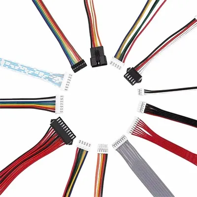
Comprehensive electrical testing is carried out to verify the electrical performance of the PCBA. This includes testing the continuity of the electrical circuits, the functionality of the components, and the signal integrity. Advanced testing equipment such as automated test equipment (ATE) and in – circuit testers (ICT) can be used to perform these tests efficiently and accurately.
Conclusion
Quick Turn PCB Assembly As a PCBA supplier, understanding the requirements for PCBA in high – pressure environments is crucial for providing high – quality products. Meeting these requirements involves careful material selection, proper design and manufacturing techniques, and rigorous testing and validation. If you are in the market for PCBA solutions for high – pressure applications, we are here to help. We have the expertise and experience to create customized PCBA products that meet your specific needs. Contact us for a procurement discussion, and let’s collaborate to develop the perfect PCBA solution for your high – pressure environment.
References
- Baker, J. P. (2018). Printed Circuit Board Materials and Manufacturing: A Practical Guide. Springer.
- Tu, K. N. (2013). Solders and Soldering in Microelectronics. Springer.
- Montrose, M. I. (2018). Printed Circuit Board Design Techniques for EMC Compliance: A Handbook for Designers. Wiley – IEEE Press.
Huaswin Electronics Technology Co., Ltd.
With abundant experience, we are one of the most professional PCBA manufacturers and suppliers in China. Welcome to wholesale customized PCBA at competitive price from our factory. If you have any enquiry about pricelist, please feel free to email us.
Address: Building A2, Hao Hai Hong Industrial Park, No.3 Yu He Road, Gong He, Sha Jing, Bao An, Shenzhen
E-mail: sales@huaswin.com
WebSite: https://www.huaswin-pcba.com/
